Here’s Everything You Need To Know About EUV Lithography

What Is Extreme Ultraviolet (EUV) Lithography?
Extreme ultraviolet (EUV) lithography is a cutting-edge technique to manufacture modern computer chips. It’s a type of photolithography, which utilises light to etch patterns onto silicon wafers, the foundation of integrated circuits (ICs).
How Does EUV Lithography Work?
EUV lithography involves an interplay of light, engineering and material science. The following is a step-by-step breakdown of the process:
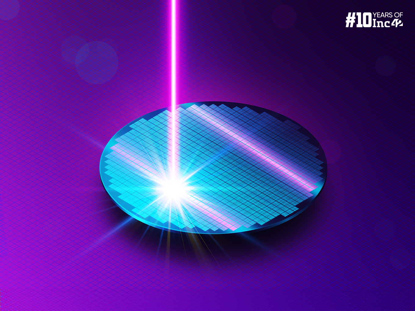
- EUV Light Source: The journey starts with generating extreme ultraviolet light. This is achieved by firing a high-powered laser at a tiny droplet of molten tin. The laser vaporises the tin, creating a hot plasma that emits EUV radiation at a specific wavelength (around 13.5 nanometres).
- Capturing Light: Air absorbs EUV light very efficiently. To overcome this hurdle, EUV systems operate in a vacuum chamber. Special mirrors with alternating layers of materials like molybdenum and silicon are used to capture and reflect the EUV light. These mirrors have an incredibly smooth and reflective surface, crucial for precise light control.
- Projecting Pattern: The captured EUV light is then projected through a photomask. This mask contains the intricate design of the circuit, with areas transparent to EUV light and others opaque. The light passing through the mask creates a sharp image of the circuit pattern onto the silicon wafer coated with photoresist.
- Exposing Resist: The photoresist reacts differently to light and shadow. Areas exposed to EUV light undergo a chemical change, making them either more or less soluble in a developer solution.
- Developing Pattern: The wafer is then bathed in a developer solution. This selectively removes the exposed (or unexposed) photoresist regions, leaving behind a relief pattern of the circuit design on the wafer.
- Etching & Cleaning: This patterned photoresist acts as a mask for subsequent etching processes. The wafer is subjected to various etching techniques to transfer the circuit design onto the underlying silicon layer. Finally, the remaining photoresist is removed, and the wafer is meticulously cleaned to prepare it for further processing.
- Repeating The Process: Creating a modern chip involves building multiple layers of circuits on the silicon wafer. This often requires repeating the EUV lithography process numerous times (up to a hundred!), each with a different photomask to create various chip components.
What Are The Advantages & Disadvantages Of EUV Lithography?
Even though EUV Lithography is one of the most advanced techniques out there, it has its benefits and drawbacks to consider:
Advantages Of EUV Lithography
- Higher Resolution: The key advantage of EUV lithography lies in its use of extremely short-wavelength light (13.5 nanometres). This allows for the creation of much finer features on the silicon wafer compared to older techniques using longer wavelengths. This translates to:
- Denser Circuits: By enabling the fabrication of smaller transistors, EUV allows for cramming more transistors onto a single chip, leading to denser and more powerful integrated circuits.
- Faster & More Efficient Chips: Denser circuits translate to faster processing speeds and improved power efficiency in the final chip.
- Improved Performance: EUV lithography can achieve higher resolution and tighter patterning than alternative lithography techniques. This leads to better performance and capabilities in the final chips.
- Potential For Future Advancements: EUV is considered essential for the continued miniaturisation of transistors, allowing the development of even more powerful and complex chips.
Disadvantages Of EUV Lithography
- Complexity & Cost: EUV systems are incredibly complex and expensive. The light source itself requires a high-powered laser and a vacuum environment. Additionally, the specialised mirrors used to capture and reflect EUV light are highly intricate and costly to manufacture. As of now, only ASML manufactures these systems commercially.
- Challenges With Materials: EUV light is highly reactive and can damage many materials commonly used in chip manufacturing. This necessitates the use of specialised materials for the photomasks, resists, and other components within the EUV system, further adding to the cost and complexity.
- Lower Throughput: Compared to deep ultraviolet (DUV) lithography, EUV currently has a lower throughput, meaning it takes longer to manufacture each wafer. This can be a bottleneck in high-volume chip production.
- Immature Infrastructure: EUV technology is still relatively new, and the supporting infrastructure for mask making, defect inspection, and yield optimisation needs to be more mature.
Is Extreme Ultraviolet (EUV) Lithography Better Than Photolithography?
EUV lithography is considered better than conventional photolithography for certain aspects of chip manufacturing, particularly when it comes to miniaturisation and finer feature size.
For high-volume chip production where cost and speed are crucial, deep ultraviolet (DUV) might still be preferred for some layers of the chip. However, for cutting-edge chips where maximising transistor density and performance is paramount, EUV becomes the necessary technology, especially for the most intricate layers of the circuit.
EUV is like a high-precision scalpel for creating the most delicate features, while DUV remains a versatile workhorse for general chip manufacturing. The choice often involves a trade-off between cost, performance, and feature size requirements.
The post Here’s Everything You Need To Know About EUV Lithography appeared first on Inc42 Media.
No comments